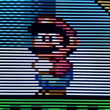
The NES PPU, or Picture Processing Unit, generates a composite video signal with 240 lines of pixels, designed to be received by a television. When the Famicom chipset was designed in the early 1980s, it was considered quite an advanced 2D picture generator for video games. It has its own address space, which typically contains 10 kilobytes of memory: 8 kilobytes of ROM or RAM on the Game Pak (possibly more with one of the common mappers) to store the shapes of background and sprite tiles, plus 2 kilobytes of RAM in the console to store a map or two. Two separate, smaller address spaces hold a palette, which controls which colors are associated to various indices, and OAM (Object Attribute Memory), which stores the position, orientation, shape, and color of the sprites, or independent moving objects. These are internal to the PPU itself, and while the palette is made of static memory, OAM uses dynamic memory (which will slowly decay if the PPU is not rendering).
Pattern Tables
The pattern table is an area of memory connected to the PPU that defines the shapes of tiles that make up backgrounds and sprites. This data is also known as CHR, and the memory attached to the PPU which contains it may either be CHR-ROM or CHR-RAM. CHR comes from "character", as related to computer text displays where each tile might represent a single letter character. Each tile in the pattern table is 16 bytes, made of two planes. Each bit in the first plane controls bit 0 of a pixel's color index; the corresponding bit in the second plane controls bit 1. The pattern table is divided into two 256-tile sections: a first pattern table at $0000-$0FFF and a second pattern table at $1000-$1FFF. Occasionally, these are nicknamed the "left" and "right" pattern tables based on how emulators with a debugger display them. An important aspect of a mapper's capability is how finely it allows bank switching parts of the pattern table. It is conventional for debugging emulators' video memory viewers to display the pattern table as two 16x16-tile grids side by side. They draw the pattern table at $0000-$0FFF on the left and the pattern table at $1000-$1FFF on the right. Each pattern table is commonly represented as a 128 by 128 pixel square, with 16 rows of 16 tiles. Usually the tiles are shown left to right, top to bottom, in Western reading order: $00 in the top left, $01 to the right of that, through $0F at the top right, then $10 through $1F on the second row, all the way through $FF at the bottom right. Some emulators have an option to rearrange the view for 8x16 sprites, where the first two rows are $00, $02, $04, ..., $1E, and $01, $03, $05, ..., $1F, and then each pair of rows below that shows another 16 pairs of tiles.
Registers
The PPU exposes eight memory-mapped registers to the CPU. These nominally sit at $2000 through $2007 in the CPU's address space, but because their addresses are incompletely decoded, they're mirrored in every 8 bytes from $2008 through $3FFF. For example, a write to $3456 is the same as a write to $2006. The PPU starts rendering immediately after power-on or reset, but ignores writes to most registers (specifically $2000, $2001, $2005 and $2006) until reaching the pre-render scanline of the next frame; more specifically, for around 29658 NTSC CPU cycles or 33132 PAL CPU cycles, assuming the CPU and PPU are reset at the same time.